共找到90條詞條名為楊濤的結果 展開
- 百度公司原副總裁
- 甘肅省慶陽市人民政府副市長
- 雲南省城市建設投資集團有限公司副董事長
- 華中科技大學能源與動力工程學院副教授
- 貴州省國家安全廳廳長、黨委書記
- 中國科學院半導體研究所研究員
- 中國書法院副研究員
- 四川金堂縣委常委
- 新東方教師
- 江蘇省人民醫院內分泌科主任
- 日海智能CEO、芯訊通&龍尚董事長
- 企業家
- 執業醫師
- 哈爾濱市呼蘭區政府副區長
- 電影導演
- 中國科技大學教授
- 上海長海醫院麻醉科副主任醫師
- 吉林厚德食品有限公司董事長兼總經理
- 鷹潭市發改委黨組成員、副主任
- 西北工業大學計算機學院副教授
- 北海市委信息綜合值班室值班科科長
- 漳縣政府副縣長
- 天津市紅橋區環保局辦公室主任
- 主任律師
- 中國書法家協會會員
- 山東淄博市武術院副院長兼散打隊總教練
- 詞曲作家
- 千人橋鎮黨委委員、副鎮長
- 邯鄲市峰峰礦區農村信用合作聯社理事長
- 攜程集團執行副總裁、旅遊事業部董事長
- 中國社科院金融學者
- 陶瓷藝術家
- 楊富智
- 億美博科技有限公司總經理
- 西藏自治區人民檢察院山南分院檢察員
- 南京市城市與交通規劃設計研究院院長
- 中國速度滑冰運動員
- 青年畫家
- 四川省綿陽市城市管理行政執法局局長
- 藝術家
- 青島科技大學教授
- 歌手
- 商務部綜合司副司長
- 中國拳擊運動員
- 棗莊市台兒庄區華陽社區志願者協會會長
- 雲南師範大學文理學院副院長
- 蕪湖市高考理科第一名
- 編劇
- 爐霍縣縣防災減災局副局長
- 贛州市人民檢察院幹部(作家)
- 福州大學兼職教授
- 河北大學化學與環境科學學院碩導
- 中國地震局地球物理研究所研究員
- 中國刑事警察學院公安基礎教研室主任、教授
- 時評作家楊濤
- 蘇寧銀行獨立董事
- 藝術工作者
- 陶瓷藝術家
- 化妝師
- 黑龍江牡丹江博大律師學院院長
- 美國加州大學教授
- 惠水縣農村合作醫療辦公室副主任
- 河海大學教授
- 陝西戶縣縣委宣傳部幹部(畫家)
- 宿州市發展和改革委員會行政審批科科長
- 醫生
- 林州市作家
- 西南交通大學講師
- 濰坊學院特教幼教師範學院舞蹈教研室教師
- 曹州青年書畫院副院長
- 原北京市通州區潞河醫院放射科大夫
- 中國郵政集團公司速遞物流專業內訓師
- 四川省瀘州市工商局黨組成員、副局長
- 商務部綜合司副巡視員
- 西北大學數學學院黨委副書記
- 巴中市工商業聯合會經濟科科長
- 荊州市發展和改革委員會紀檢組組長
- 深圳青年歌唱家
- 寧夏第五建築有限公司第五項目部項目經理
- 西安知象光電CTO
- 實習律師
- 鶴慶縣政府辦公室副主任
- 中國石油化工股份有限公司洛陽分公司煉油三部焦化二班班長
- 銀川市水產技術推廣服務中心司機
- 荊州市第一人民醫院臨床三黨支部宣傳紀檢委員、神經內科醫師
- 中國平安保險公司行銷主任
- 蔚縣審計局駐蔚縣西方城村工作隊員
- 中國農業銀行邯鄲肥鄉支行行長
- 攝影師
- 商業人物
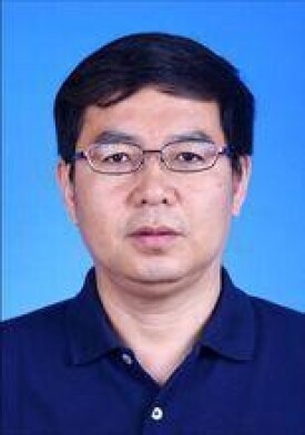
楊濤
中國科學院半導體研究所研究員
楊濤,研究員,博士生導師, 中科院“百人計劃”入選者。1997年畢業於日本德島大學,獲工學博士。博士畢業后,作為研究員或助理教授曾先後任職於日立公司中央研究所,新能源產業技術綜合開發機構(NEDO)和東京大學。2006年,作為中科院“引進海外傑出人才”回國到半導體研究所工作。
楊濤博士長期從事半導體材料、器件與物理研究,尤其在氮化物半導體新材料、光子晶體和納米結構半導體量子點材料及器件應用等前沿領域中取得了多項創新性成果。
1)理論上建立了適於III族氮化物半導體電子能帶結構計算的緊束縛近似模型。該模型被國際同行稱作“標準的緊束縛近似模型”;
2)基於此模型給出了III族氮化物合金材料的能帶圖、禁帶、電子有效質量等表徵其物理特性的重要物理量。這些物理量對基於III族氮化物半導體材料的光電子器件的設計與模擬,材料物理特性的實驗研究等具有重要意義;
3)理論上證明了V族立方相氮化物合金(InAsN)具有大的帶隙彎曲參量,預言此材料可作為發展長波長信息功能器件的新材料;
4)提出了“高溫緩衝層”概念,用“三步生長法”取代“傳統的兩步生長法”在藍寶石襯底上用MOCVD製備出高質量GaN晶體。這對於發展GaN基的光電子器件具有重要的現實意義;
5)近年,主要致力於低維半導體量子點材料與器件應用的研究並取得了一系列成果:如,在國際上證明了最均勻的1.3微米輻射InAs/GaAs自組織量子點材料(非均勻展寬<17 meV);報道了快速退火能使長波長量子點產生大的波長藍移現象,闡明了產生這一現象的物理機理;在國內實現了無外部致冷、高速(10 Gb/s)、直接調製的1.3微米GaAs基量子點激光器,報道了基於InAs/GaAs量子點材料的中間能帶太陽能電池等。
1)國家重大科學研究計劃項目“新型半導體納米線的可控生長和表徵” (2012-2016);
2)國家自然科學基金項目“基於MOCVD高性能1.55微米InAs/InP自組織量子點材料生長及激光器應用研究”(2012-2015);
3)國家自然科學基金項目“新型高效InAs/GaAs量子點中間能帶太陽能電池的研究”(2011-2013);
4)國家自然科學基金項目“新型P型摻雜1.3微米InAs/GaAs自組織量子點材料生長及激光器應用相關基礎研究”(2009-2011);
5)中科院百人計劃項目“低維半導體量子點材料和器件應用研究”(2007-2010);
6)國家863計劃項目“新型P型摻雜GaAs基1.3微米InAs量子點激光器研究”(2006.12 - 2008.12)。
1) P. F. Xu, H. M. Ji, T. Yang*, B. Xu, W. Q. Ma, and Z. G. Wang, “The Research Progress of Quantum Dot Lasers and Photodetectors in China”, Journal of Nanoscience and Nanotechnology, Vol.11(2011), pp. 9345-9356.
2) Y. X. Gu, T. Yang*, H. M. Ji, P. F. Xu, and Z. G. Wang, “Redshift and discrete energy level separation of self-assembled quantum dots induced by stain-reducing layer”, J. Appl. Phys. Vol. 109 (2011), pp. 064320-064324.
3) P. F. Xu, T. Yang*, H. M. Ji, Y. L. Cao, Y. X. Gu, and Z. G. Wang, “Temperature compensation for threshold current and slope efficiency of 1.3 mm InAs/GaAs quantum-dot lasers by facet coating design”, Chin. Phys. Lett. Vol. 28 (2011) pp. 044201-044203.
4) X. G. Yang, T. Yang*, K. F. Wang, Y. X. Gu, H. M. Ji, P. F. Xu, H. Q. Ni, Z. C. Niu, X. D. Wang, Y. L. Chen, and Z. G. Wang, “Intermediate-band solar cells based on InAs/GaAs quantum dots”, Chin. Phys. Lett. Vol. 28 (2011) pp. 038401-038403.
5) H. M. Ji, T. Yang*, Y. L. Cao, P. F. Xu, Y. X. Gu, and Z. G. Wang, “Self-Heating Effect on the Two-State Lasing Behaviors in 1.3 μm InAs–GaAs Quantum-Dot Lasers”, Jpn. J. Appl. Phys. Vol. 49 (2010) pp. 072103-072106.
6) Y. L. Cao, T. Yang*, P. F. Xu, H. M. Ji, Y. X. Gu, X. D. Wang, Q. Wang, W. Q. Ma, Q. Cao, and L. H. Chen, “Delay of the excited state lasing of 1310 nm InAs/GaAs quantum dot lasers by an optimal facet coating”, Appl. Phys. Lett. Vol.96 (2010) pp. 171101-171103.
7) H. M. Ji, T. Yang*, Y. L. Cao, P. F. Xu, Y. X. Gu, Y. Liu, L. Xie, and Z. G. Wang, “A 10 Gb/s directly-modulated 1.3 μm InAs/GaAs quantum-dot Laser”, Chin. Phys. Lett. Vol. 27 (2010) pp. 034209-034211.
8) H. M. Ji, T. Yang*, Y. L. Cao, P. F. Xu, Y. X. Gu, W. Q. Ma, and Z. G. Wang, “High characteristic temperature 1.3 μm InAs/GaAs quantum-dot lasers grown by molecular beam epitaxy”, Chin. Phys. Lett. Vol. 27 (2010) pp. 027801-027803.
9) P. F. Xu, T. Yang*, H. M. Ji, Y. L. Cao, Y. X. Gu, Y. Liu, W. Q. Ma, and Z. G. Wang, “Temperature-Dependent Modulation Characteristics for 1.3 mm InAs/GaAs Quantum Dot Lasers”, J. Appl. Phys. Vol.107 (2010) pp. 013102- 013106.
10) Y. L. Cao, T. Yang*, H. M. Ji, W. Q. Ma, Q. Cao, and L. H. Chen, “Temperature sensitivity dependence on cavity length in p-type doped and undoped 1.3 mm InAs/GaAs quantum dot lasers”, IEEE Photon. Technol. Lett. Vol. 20 (2008) pp. 1860-1862.
11) T. Yang, J. Tatebayashi, K. Aoki, M. Nishioka, and Y. Arakawa, “Effects of rapid thermal annealing on the emission properties of highly uniform self-assembled InAs/GaAs quantum dots emitting at 1.3 µm”, Appl. Phys. Lett. Vol.90 (2007) pp. 111912- 111914.
12) T. Yang, J. Tatebayashi, M. Nishioka, and Y. Arakawa, “Improved surface morphology of stacked 1.3 µm InAs/GaAs quantum dot active regions by introducing annealing processes”, Appl. Phys. Lett. Vol.89 (2006) pp. 081902-081904.
13) T. Yang, S. Tsukamoto, J. Tatebayashi, M. Nishioka, and Y. Arakawa, “Improvement of the uniformity of self-assembled InAs quantum dots grown on InGaAs/GaAs by low-pressure metalorganic chemical vapor deposition”, Appl. Phys. Lett. Vol.85 (2004) pp. 2753-2755.
14) T. Yang, J. Tatebayashi, S. Tsukamoto, M. Nishioka, and Y. Arakawa, “Narrow photoluminescence linewidth (< 17 meV) from highly uniform self-assembled InAs/GaAs quantum dots grown by low-pressure metalorganic chemical vapor deposition”, Appl. Phys. Lett. Vol.84 (2004) pp. 2817-2819.
15) T. Yang, Y. Sugimoto, S. Lan, N. Ikeda, Y. Tanaka, and K. Asakawa, “Transmission properties of coupled cavity waveguides based on two-dimensional photonic crystals with a triangular lattice of air holes”, J. Opt. Soc. Am. B Vol.20 (2003) pp. 1922-1926.
16) T. Yang, S. Kohmoto, H. Nakamura, and K. Asakawa, “Effects of lateral quantum dot pitch on the formation of vertically aligned InAs site-controlled quantum dots”, J. Appl. Phys. Vol.93 (2003) pp. 1190-1194.
17) T. Yang, T. Ishikawa, S. Kohmoto, Y. Nakamura, H. Nakamura, and K. Asakawa, “Height control of InAs/GaAs quantum dots by combining layer-by-layer in situ etching and molecular beam epitaxy”, J. Vac. Sci. Technol. B Vol. 20 (2002) pp. 668-672.
18) T. Yang, K. Uchida, T. Mishima, J. Kasai, and J. Gotoh, “Control of initial nucleation by reducing the V/III ratio during the early stage of GaN growth”, Phys. Status Solidi (a) Vol. 180 (2000) pp. 45-50.
19) T. Yang, S. Goto, M. Kawata, K. Uchida, A. Niwa, and J. Gotoh, “Optical properties of GaN thin films on sapphire substrates characterized by variable-angle spectroscopic ellipsometry”, Jpn. J. Appl. Phys., Part 2 Vol. 37 (1998) pp. L1105-L1108.
20) T. Yang, S. Nakajima, and S. Sakai, “Tight-binding calculation of electronic structures of InNAs ordered alloys”, Jpn. J. Appl. Phys., Part 2 Vol. 36 (1997) pp. L320-L322.
21) T. Yang, S. Nakajima, and S. Sakai, “Electronic structures of wurtzite GaN, InN and their alloy Ga1-xInxN calculated by the tight-binding method”, Jpn. J. Appl. Phys., Part 1 Vol. 34 (1995) pp. 5912-5921.
基本信息
- 中文名
- 楊濤
- 國籍
- 中國
- 性別
- 男
- 職業
- 研究員